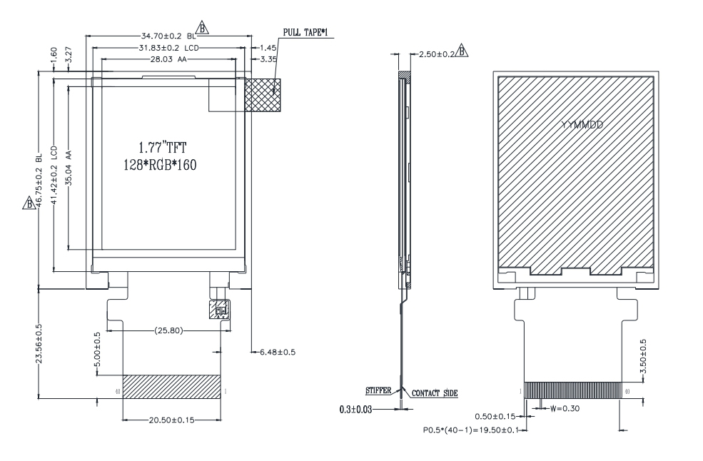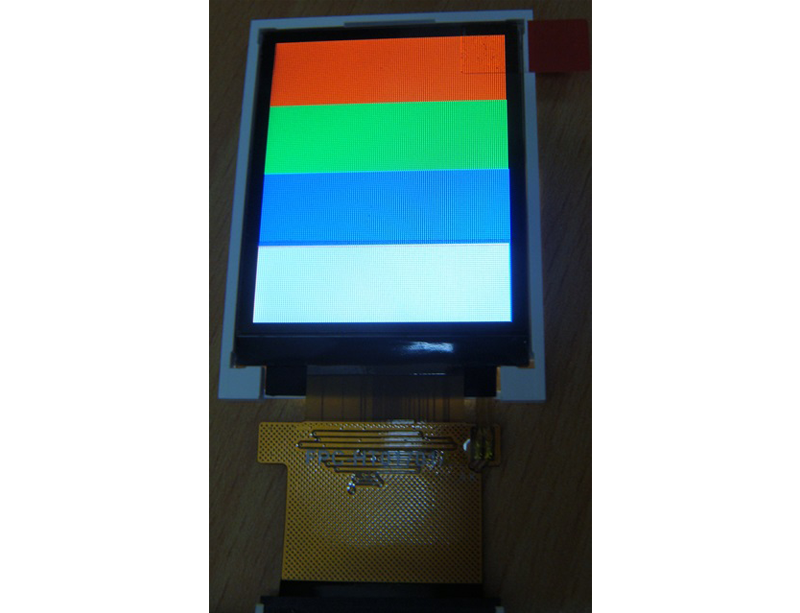
| Pin No | Symbol | Description |
|---|---|---|
| 1 | LED- | LED cathode |
| 2 | LED+ | LED anode |
| 3~4 | IM0~IM1 | MCU Parallel Interface Type Selection |
| 5 | IM2 | IM2=’1’, Parallel Interface IM2=’0’, Serial Interface If Not Used, Please Fix this Pin at VDDI or DGND Level |
| 6 | RESET | Reset signal input |
| 7 | SPI4W | SPI4W=’0’, 3-line SPI Enable SPI4W=’1’, 4-line SPI Enable If Not Used, Please fix this Pin at DGND |
| 8~12 | NC | No Connect |
| 13~27 | DB15~DB1 | Data bus |
| 28 | DB0(SDA) | Data bus, DB0 is the serial data input/output signal in serial interface mode |
| 29 | NC | No Connect |
| 30 | RD | Read Enable in 8080 MCU Parallel Interface. |
| 31 | W/R(D/C) | Write Enable in MCU Parallel Interface. In 4-line SPI, this pin is used as D/CX (data/ command selection). If not used, please fix this pin at VDDI or DGND level. |
| 32 | D/C(SCL) | D/CX=’1’: Display Data or Parameter. D/CX=’0’: Command Data. In Serial Interface, this is used as SCL. If not used, please fix this pin at VDDI or DGND level |
| 33 | CS | Chip Selection Pin; Low Enable |
| 34 | IOVCC | Power Supply for I/O system |
| 35 | VCI | Power Supply |
| 36 | VSS | Ground |
| 37~40 | NC | No Connect |